
Micron's DeBoer: G11 NAND brings wafer bonding and 5,400 MT/s speeds by 2027
The company plans to use wafer-on-wafer bonding to double storage capacity and boost I/O speeds by 50% for data centers and AI workloads.
By Thomas Rogers ·
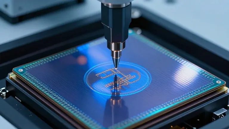
Micron will begin mass production of its G11 3D NAND flash in the second half of 2027. The new generation doubles the storage density of the current lineup, moving from 21 Gb/mm2 to 42 Gb/mm2 in triple-level-cell form. This capacity increase allows the company to meet rising demand for high-bandwidth storage in artificial intelligence applications.
The performance gains extend beyond raw capacity. I/O speeds will rise by up to 50%, increasing from 3,600 MT/s to 5,400 MT/s. Energy consumption per bit will drop by more than 25%. These improvements make the chips suitable for conventional high-capacity SSDs used in client devices and data centers, as well as specialized storage for AI workloads.
A key manufacturing change drives these specifications. Micron will adopt wafer-on-wafer bonding for the first time. This method separates the production of the memory array and the peripheral circuitry. Each component is built on a different wafer using a process optimized for its specific function before the two are bonded together. This approach provides more freedom to optimize both the memory and logic sections independently.
Scott DeBoer, Micron’s president and chief technology and products officer, confirmed the shift to this technology. "This is the right timing for that technology," DeBoer said. He described G11 as the world’s most advanced NAND, noting that the company had previously promised to introduce the method when it became cost-effective.
The design will exceed 400 layers, though Micron has not disclosed the exact number of active wordlines or memory decks. The density gain comes from a combination of added layers and a smaller memory cell pitch. The company plans to release detailed technical specifications in 2027, closer to the start of high-volume production.
Looking past G11, Micron states it will continue scaling in all three dimensions. The company is developing high-mobility materials and ultra-dense cell architectures to improve transistor characteristics and reduce energy use. DeBoer noted that the roadmap focuses on new materials and continued XYZ scaling, without providing specific dates or density targets for future generations.
Source: Tom's Hardware